TL;DR
A hardware hacker has successfully demonstrated a direct, low-latency method for running PCI Express (PCIe) devices over fiber optic cables using standard SFP+ modules, bypassing the need for encapsulating protocols like Thunderbolt. This proof-of-concept, published on April 11, 2026, could significantly lower the cost and complexity of external high-speed computing setups for AI accelerators, GPUs, and storage arrays, challenging the dominance of proprietary commercial solutions.
What Happened
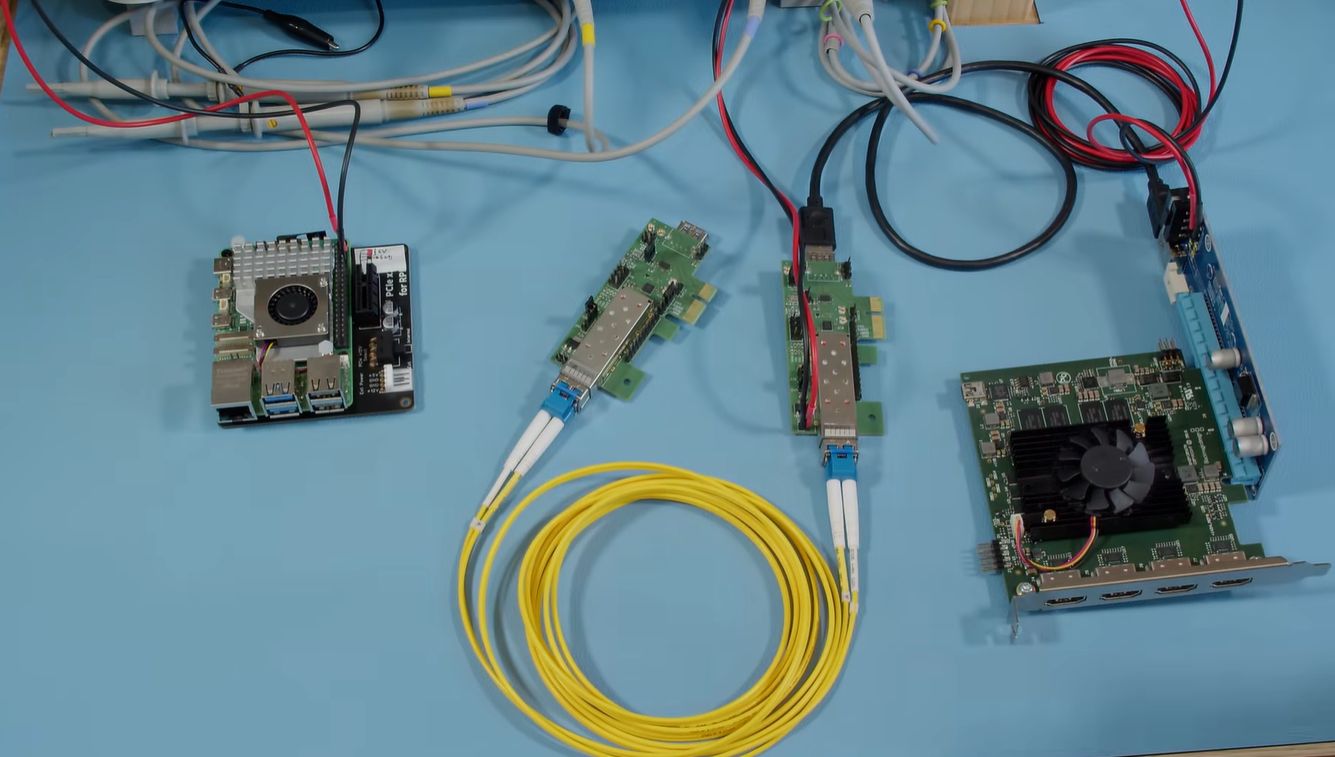
On Saturday, April 11, 2026, the hardware engineering community site Hackaday published a detailed project log showcasing a groundbreaking technical achievement. An independent developer has successfully built a functional proof-of-concept system that transmits raw PCI Express (PCIe) signals over fiber optic cabling, using readily available SFP+ (Small Form-factor Pluggable) optical transceivers. This direct approach bypasses the protocol overhead and licensing costs of commercial external GPU enclosures, which rely on technologies like Thunderbolt to encapsulate and transport PCIe data.
Key Facts
- Source & Date: The project was documented in a comprehensive article on Hackaday, published on Saturday, April 11, 2026.
- Core Innovation: The project implements PCIe over fiber directly, avoiding encapsulating protocols like Thunderbolt or Ethernet used in commercial products.
- Key Hardware: The system leverages standard, off-the-shelf SFP+ optical modules and fiber cables for the physical layer data transmission.
- Target Applications: The primary use case is for externalizing high-bandwidth PCIe devices, specifically mentioned are GPUs, outside of a traditional PC chassis.
- Market Context: This DIY method presents a potential low-cost, low-latency alternative to existing commercial external PCIe solutions, which are often expensive and tied to specific vendor ecosystems.
Breaking It Down
This project represents a significant leap in democratizing high-performance, disaggregated computing. While companies like Intel (with Thunderbolt) and others have created commercial, consumer-friendly products for external PCIe devices, they add layers of protocol conversion, introduce latency, and come with substantial cost premiums. The Hackaday contributor’s work strips this back to the essentials, treating the PCIe lanes as a raw, high-speed serial stream that can be pushed directly over fiber optics—a medium inherently suited to the task due to its high bandwidth and noise immunity.
The most striking implication is the potential for sub-microsecond, protocol-agnostic latency for external devices, a critical factor for real-time AI inference and high-frequency trading applications where Thunderbolt's overhead is a bottleneck.
By eliminating the Thunderbolt controller's need to packetize PCIe transactions into a DisplayPort-compatible data stream, this direct fiber link could achieve near-native PCIe latency. For workloads like AI model inference on external accelerators or latency-sensitive financial computations, shaving off even tens of microseconds can translate to tangible performance gains and cost savings. This makes the technique particularly compelling for niche, high-performance computing (HPC) and research applications where commercial solutions are either too slow or too expensive.
The technical hurdle overcome here cannot be understated. PCIe is a complex, high-speed, differential electrical signaling standard not designed for long-distance transmission. The developer’s work involved designing or adapting circuitry to perform the critical electrical-to-optical conversion at the PCIe lane level, likely using retimer or redriver chips to condition the signal before it enters the SFP+ module. This is distinct from simply running PCIe over Ethernet (which requires full protocol encapsulation), making it a purer, more direct pipe for the PCIe protocol itself.
Furthermore, this development challenges the economic model of external expansion. A commercial Thunderbolt or proprietary external PCIe chassis can cost hundreds of dollars before adding the cost of the card itself. A DIY fiber link, built from commodity SFP+ modules, fiber cables, and custom PCBs, could theoretically be assembled for a fraction of that cost, opening the door for bespoke server farms, render nodes, or lab setups that physically separate CPUs from pools of accelerators and storage.
What Comes Next
The publication of this proof-of-concept is a starting pistol, not a finish line. It immediately catalyzes several avenues of development and scrutiny within the open-source hardware and enterprise IT communities.
- Community Validation and Refinement (Next 3-6 months): The immediate next step is for other hardware experts to replicate, test, and benchmark the design. Key metrics to be validated include maximum stable link length, supported PCIe generation (e.g., Gen 3 vs. Gen 4), lane width (x4, x8, x16), and real-world latency measurements compared to Thunderbolt 4 or 5. The Hackaday project page will likely become a forum for iterative design improvements.
- Commercial Open-Source Hardware Kits (Late 2026 - 2027): It is highly probable that enterprising open-source hardware firms or community members will develop and sell refined PCB kits, pre-programmed FPGAs, or turn-key adapter boards. This would lower the barrier to entry from "advanced hardware hacker" to "enthusiast with soldering skills," potentially creating a new niche market for DIY external expansion.
- Exploration of New Architectures (2027 and beyond): Successful validation will spur research into more ambitious applications. This includes designing PCIe switching fabrics over optical backplanes for modular compute racks, or creating ultra-low-latency links for computational storage drives (CSDs) and CXL (Compute Express Link) devices in memory-dense systems, pushing the boundaries of data center disaggregation.
The Bigger Picture
This innovation dovetails with two powerful, ongoing trends in technology. First, it accelerates the move toward disaggregated and composable infrastructure. The traditional model of a monolithic server with fixed resources is being challenged by architectures where CPU, memory, storage, and accelerators are separate, poolable resources. A reliable, low-latency method to place a GPU dozens of meters away from its host CPU via simple fiber is a concrete step toward this flexible future, especially for small-scale clusters and edge computing.
Second, it represents a pushback against proprietary peripheral ecosystems. Thunderbolt, while powerful, is an Intel-controlled standard with licensing fees. USB4, while more open, still involves protocol conversion. This direct PCIe-over-fiber hack exemplifies a growing desire in the developer and enterprise communities for open, high-performance interconnects that are not tied to a single vendor's roadmap or business model. It echoes the ethos behind open standards like PCIe itself, applying it to the problem of physical device placement.
Key Takeaways
- Direct PCIe Transmission: A functional method for running native PCIe signals over fiber optics has been demonstrated, bypassing the need for Thunderbolt encapsulation.
- Latency & Cost Advantage: The approach promises lower latency and potentially lower cost than commercial external GPU/enclosure solutions, targeting performance-critical applications.
- Open Hardware Potential: This is primarily an open-source hardware breakthrough, challenging proprietary solutions and enabling community-driven development of external expansion technology.
- Niche to Mainstream Pathway: While currently a complex DIY project, it lays the groundwork for future commoditized kits and novel data center architectures based on physically separated compute resources.